Chapter 1. Impact 8.5
Impact …ON NANOSCIENCE: I8.5 Nanowires
Research on nanometre-sized materials is motivated by the possibility that they will form the basis for cheaper and smaller electronic devices. The synthesis of nanowires, nanometre-sized atomic assemblies that conduct electricity, is a major step in the fabrication of nanodevices. An important type of nanowire is based on carbon nanotubes, which, like graphite, can conduct electrons through delocalized π molecular orbitals that form from unhybridized 2p orbitals on carbon. Recent studies have shown a correlation between structure and conductivity in single-walled nanotubes (SWNTs) that does not occur in graphite. The SWNT in Fig. 1 is a semiconductor. If the hexagons are rotated by 90° about their sixfold axis, the resulting SWNT is a metallic conductor.
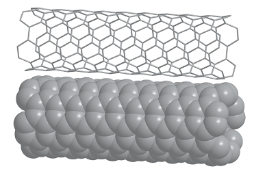
Fig. 1. In a single-walled nanotube (SWNT), sp2-hybridized carbon atoms form hexagonal rings that grow as tubes with diameters between 1 and 2 nm and lengths of several micrometres.
Carbon nanotubes are promising building blocks not only because they have useful electrical properties but also because they have unusual mechanical properties. For example, an SWNT has a Young’s modulus that is approximately five times larger and a tensile strength that is approximately 375 times larger than that of steel.
Silicon nanowires can be made by focusing a pulsed laser beam on to a solid target composed of silicon and iron. The laser ejects Fe and Si atoms from the surface of the target, forming a vapour that can condense into liquid FeSin nanoclusters at sufficiently low temperatures. The phase diagram for this complex mixture shows that solid silicon and liquid FeSin coexist at temperatures above 1473 K. Hence, it is possible to precipitate solid silicon from the mixture if the experimental conditions are controlled to maintain the FeSin nanoclusters in a liquid state that is supersaturated with silicon. It is observed that the silicon precipitate consists of nanowires with diameters of about 10 nm and lengths greater than 1 μm.
Nanowires are also fabricated by molecular beam epitaxy (MBE), in which gaseous atoms or molecules are sprayed on to a crystalline surface in an ultra-high vacuum chamber. The result is formation of highly ordered structures. Through careful control of the chamber temperature and of the spraying process, it is possible to deposit thin films on to a surface or to create nanometre-sized assemblies with specific shapes. For example, Fig. 2 shows an image of germanium nanowires on a silicon surface. The wires are about 2 nm high, 10–32 nm wide, and 10–600 nm long.
Fig. 2. Germanium nanowires fabricated on to a silicon surface by molecular beam epitaxy. The images were obtained by atomic force microscopy, a technique described in Topic 95. (Reproduced with permission from T. Ogino et al., Acc. Chem. Res. 32, 447 (1999).)